|
|
|
Архитектура Астрономия Аудит Биология Ботаника Бухгалтерский учёт Войное дело Генетика География Геология Дизайн Искусство История Кино Кулинария Культура Литература Математика Медицина Металлургия Мифология Музыка Психология Религия Спорт Строительство Техника Транспорт Туризм Усадьба Физика Фотография Химия Экология Электричество Электроника Энергетика |
The temperature Variation of Conductivity and Carrier Concentration.
Variation of Conductivity and Carrier Concentration Temperature causes electrons to be promotedto the conduction band and from donor levels, or holes to acceptor levels.The dependence of conductivity on temperature is like other thermally activated processes: σ =σ0 exp (-Е/2kТ), where A is a constant (the mobility varies much more slowly with temperature). Extrinsic semiconductors have, in addition to this dependence, one due to the thermal promotion of electrons from donor levels or holes from acceptor levels. The dependence on temperature is also exponential but it eventually saturates at high temperatures where all the donors are emptied or all the acceptors are filled. This means that at low temperatures, extrinsic semiconductors have larger conductivity than intrinsic semiconductors. At high temperatures, both the impurity levels and valence electrons are ionized, but since the impurities are very low in number and they are exhausted, eventually the behavior is dominated by the intrinsic type of conductivity. a) For n-tvpes-r. we can write: σ =σ0 exp -(Eg –Ed)/(kT), where Eg = bottom of conduction band; Ea = donor level.
Fig.17.5. Energy band structure of an n-type semi-conductor. The extra electron from the group VA dopant produces a donor level (Ed) near the conduction band. This provides relatively easy production of conduction electrons.
b) For p-tvpe s-r we can write Arrhenius equation: σ =σ0 exp(-Eg/kT) where Eg is acceptor level from Fig. 17.8. Fig. 17.8 shows the Arrhenius plot of Inσ versus 1/T for a p-type material. It is quite similar to Fig. 17.8 for n-type. The plateau in conductivity between the extrinsic and intrinsic regions is termed the saturation range for p-type behavior rather than exhaustion range. Saturation occurs when all acceptors levels (= number of group III A atoms) have become occupiedwith electrons.
Fig. 17.9. Energy band structure of a p-type semiconductor. The deficiency of valence electrons in the group ША dopant produces an acceptor level (Ea) near the valence band. Electron holes are produced as a result of thermal promotion over this relatively small energy barrier.
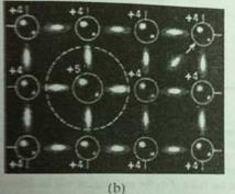
Fig. 17.10 Schematic of the production of an electron hole in a p-type semiconductor, (a) The deficiency in valence electrons for the group IIIA atom creates an empty state, or electron hole, orbiting about the acceptor atom, (b) The electron hole becomes a positive charge carrier as it leaves the acceptor atom behind with a filled acceptor state. (The motion of electron holes, of course, is due to the cooperative motion of electrons.)
Поиск по сайту: |